It-fab
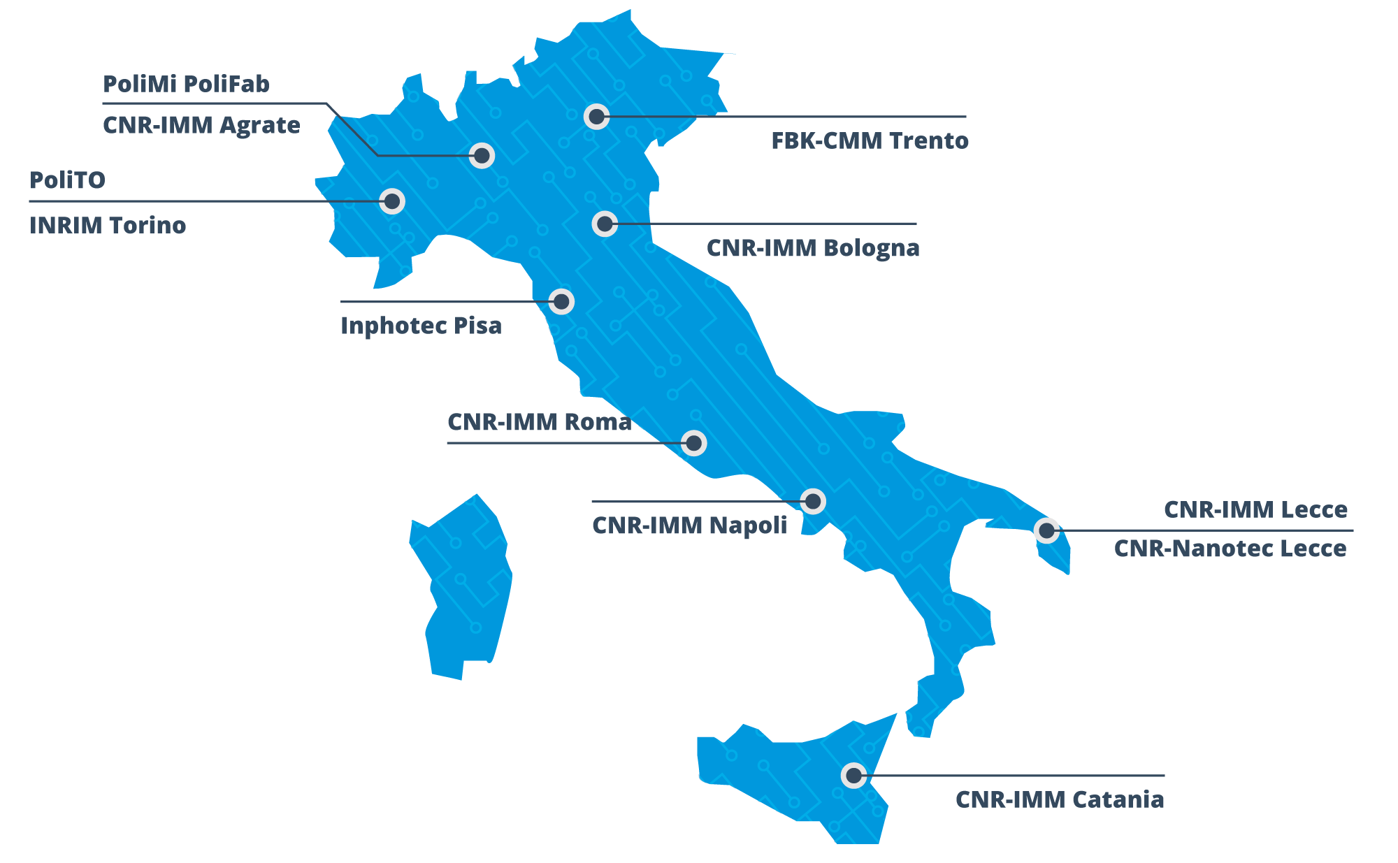
The Italian Network for Micro and Nano Fabrication
Network of Leading Institutions and Laboratories
CNR Institute for Microelectronics and Microsystems
Director: Vittorio Privitera
Contact person: Vittorio Morandi
About 44% of laboratory area is ISO6 class or better About 30% is ISO5 class (Including corridors and grey areas: >2500m2). More than 60 researchers/technicians.
Activities from fundamental studies to applied researches at high TRL and, if required, by a small scale prototype production.
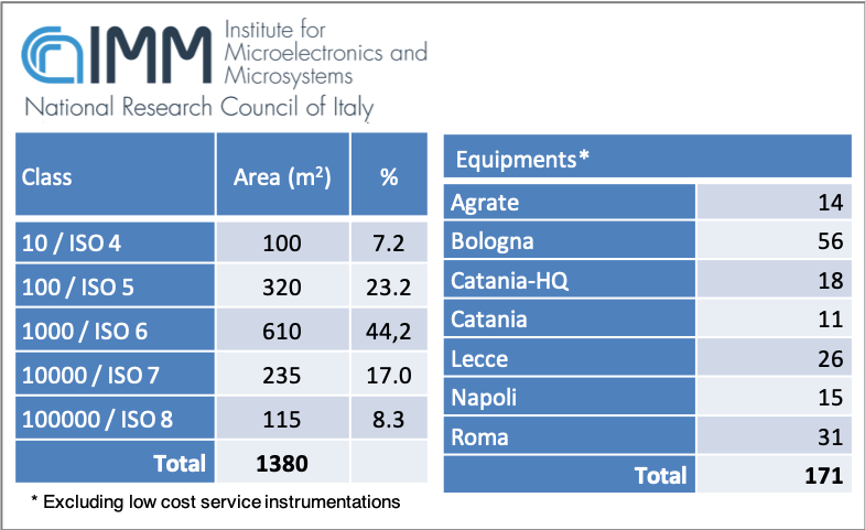
- Micro/nano lithography and Wafer bonding
- Electron and Ion beam assisted nanofabrication
- Growth, Deposition and Thermal Processes
- Etching, Cleaning and Polishing
- High and Low energy Ion Implantation
- Packaging, Metrology and Control
Substrate sizes:
- 4": complete line
- 6": almost complete
- > 8" and large area: some new or special equipment
CNR Institute of Nanotechnology
Director: Prof. Giuseppe Gigli
Contact person: Massimo Cuscunà
- 12.000 m2 labs
- 800 m2 fully equipped Clean Rooms (class 100-100000)
- 120 Researchers (Physics, Chemistry, Biology, Medicine and Engineering)
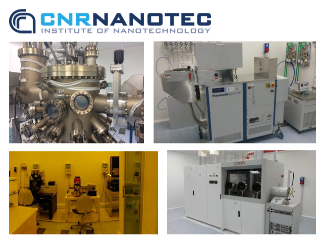
Growth Techniques of Semiconductors
- MBE: GaAs family
- MOCVD: GaN
Oxides, Silicon Nitride and Metals
- e-beam evaporator and Sputtering
- PECVD and ALD for Oxides
Nanofabrication Tools based on High-Res Lithography
- Dual Beam FIB/SEM
- High Resolution EBL
- Laser Lithography
- Class 1000 Lithography Rooms
Dry Etching Processes
- Reactive Ion Etching
- Deep-Reactive Ion Etching
FBK Micro Nano Facility
Director: Dr. Gian Luigi Casse
Contact person: Vittorio Guarnieri and Lorenza Ferrario
More then 100 people: technical staff, researchers, PhD students, startups
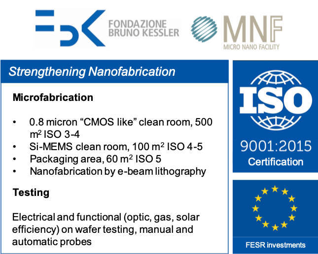
Applications Market Area/R&D specializations:
- Radiation Sensors
- MEMS
- Silicon micro-devices in fields such as particle detection, transduction, RF, optics, microfluidics, optoelectronics
- Materials analysis
- Analytical methodology development
- Analytical instrumentation development
Skills:
- Micro device development
- Materials Science
- Silicon technology
- Complex microfabrication and analytical tool management
- Workflow organization (ISO certification)
Politecnico of Milan - PoliFab
Director: Prof. Riccardo Bertacco
Contact Person: Riccardo Bertacco
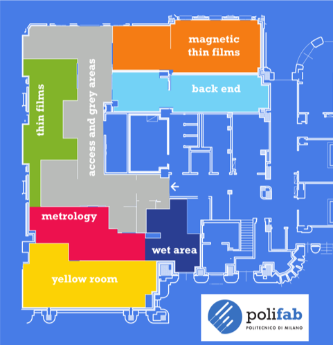
Clean Room Facility:
- 150 m2, class ISO 6
- 220 m2, class ISO 8
- 6" wafers
The clean room, is divided into two adjacent areas: the first one is a class ISO 6 (150 m2) equipped with facilities for:
- optical lithography
- electron beam lithography
- wet and dry etching
- thin film deposition
- metrological characterization
The second area is a class ISO 8 220 m2 clean room which includes:
- access and grey areas
- back-end
- magnetic thin films area
A third ISO 6 area of 200 m2 is under construction to host a Joint Research Centre with STMicroelectronics on MEMS technologies.
Inphotec Foundation
Director: Massimo Gentili
Contact Person: Alessandro Nottola
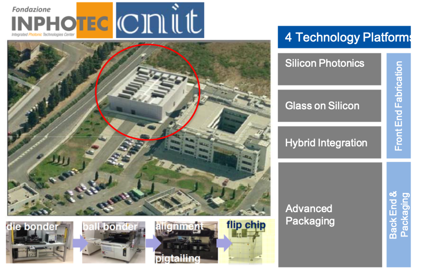
700 m2 cleanroom space
- 40 m2 class 100 ISO 5
- 190 m2 class 1000 ISO 6
- 320 m2 class 10000 ISO 7
- 150 m2 service area
Strategic plan for 2019 and beyond
- Graphene-Silicon Photonics
- Quantum Photonics
- Space Photonics
- (Bio)sensing
Advanced automated pilot line for packaging
PiQuET Piemonte Quantum Enabling Technology
Coordinators: Davide Calonico, Candido Fabrizio Pirri, Paolo Olivero
Contact Persons: Matteo Cocuzza, Giulia Aprile
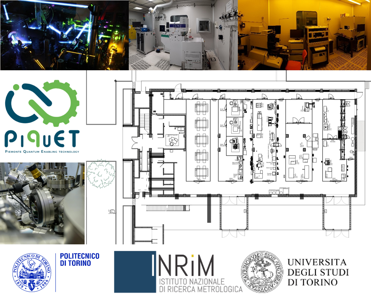
PiQuET is a facility focused on micro-nanofabrication and quantum communication/sensing (Q-Comm e Q-sense) advanced research and technological transfer with a staff of 70 researchers, technicians and PhD students.
- 33 m2 class 100 ISO 5
- 280 m2 class 1000 ISO 6
- 100 m2 class 10000 ISO 7
- 400 m2 service area and labs
- Quantum comm & metrological characterization lab
- Additive manufacturing lab
The clean room is divided in 7 areas.
- Q-Tech – Quantum devices
- Microscopy and electron/ion-beam lithography
- Etching, growth, thermal treatment
- Deposition
- Chemical
- Optical lithography
- Transmission electron microscopy
Skills: Quantum communication, quantum clocks, quantum electronics, MEMS & laser micromachining, microfluidics & Lab on chip, organ-on-chip, additive manufacturing, energy & environment, electronic biosensing, simulations & modelling.
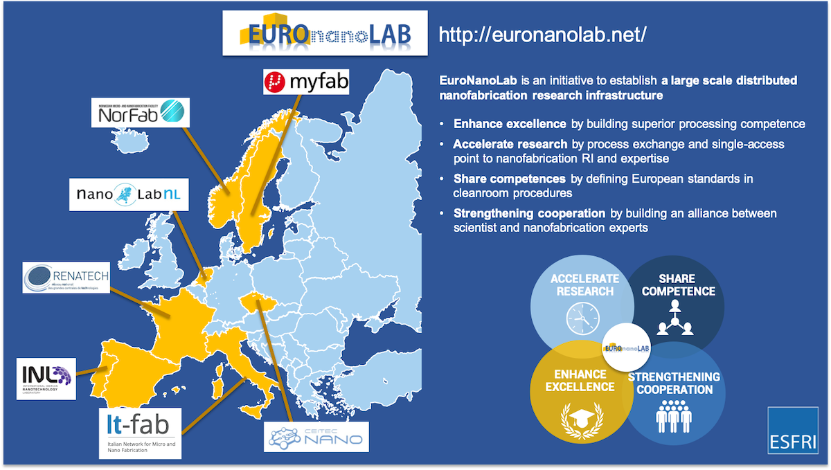
Aim and Scope
European Coordination Level
Current situation and challenges
- Fragmented national sites network
- Sites distribution not purposefully designed to address European scale issues
Impact of EuroNanoLab
- Additional national and regional focus
- Clear common goals and coordinated site distribution
It-Fab Project impact:
- Cutting-edge micro and nanofabrication facilities for the manufacture of microelectronic devices and microsystems both for industrial and for research purposes.
- Conventional microelectronic production equipment is combined with large area electronics processes to meet the needs of scholars, innovators and entrepreneurs that want to investigate new device properties or boost new applications into the market.
- A network infrastructure, distributed across Italy, could provide an optimal interface towards the national industrial tissue, mainly composed of SME.
EuroNanoLab at a Glance
Steering Committee
Coordinator: Vittorio Morandi
Project Activities
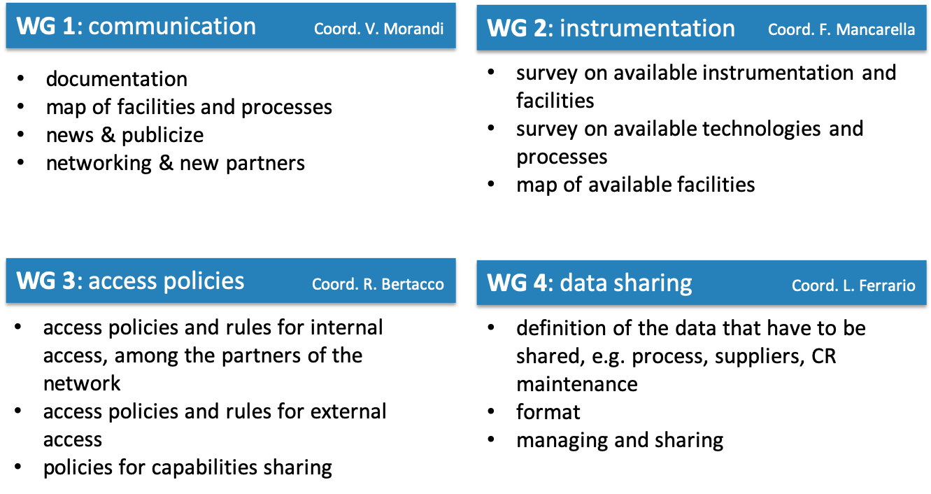
Work Groups
School on nanotechnologies: processes and applications to sensors and actuators
In the “European Strategy for Key Enabling Technologies”, the EU has defined six Key Enabling Technologies (KET): (1) micro- and nanoelectronics, (2) nanotechnology, (3) industrial biotechnology, (4) advanced materials, (5) photonics and (6) advanced manufacturing technologies, with a strong and well documented global impact. Most of these KETs require state-of-the-art facilities and competence on micro and nano-fabrication, a key area of science and technology that is radically changing our world.
The school is dedicated to Master degree and Ph.D students, as well as to scientists working in the wide field of micro- and nano-technology, offering the opportunity to learn about fundamentals on processes, devices fabrication and characterization processes, with attention to both planar and 3D technologies. Besides the lectures dedicated to single technology steps, building blocks of the silicon-based micro- and nano-fabrication technologies, there will be sessions dedicated to devices application areas. The workshop will be completed with a demo and live sessions from different cleanrooms, to practically show some of the fundamental silicon processing steps. .
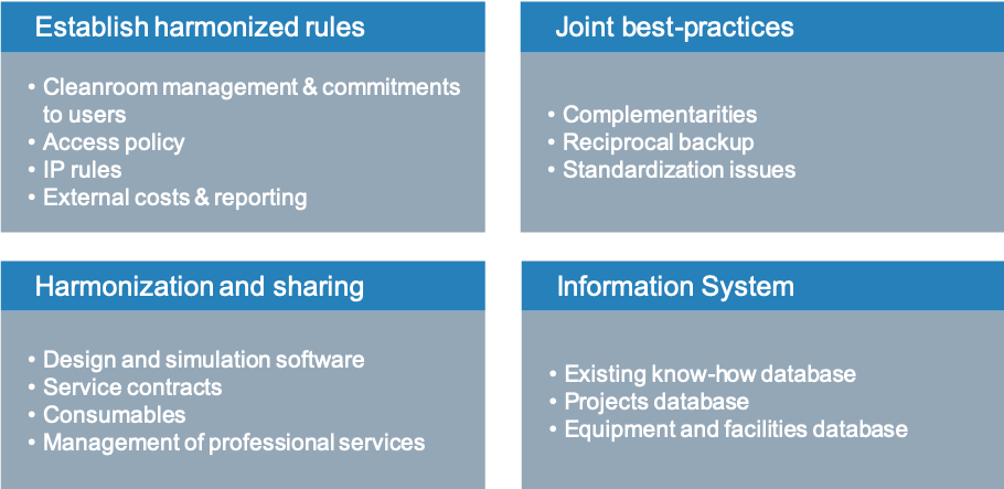
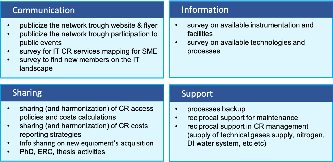
The school is organized by It-fab (http://itfab.bo.imm.cnr.it/), the Italian network for Micro and Nano Fabrication research infrastructures, an initiative that aims to (i) establish harmonized rules, for clean room management and access policies, IP rules, external costs and reporting, (ii) harmonize and share design and simulation software, service contracts, management of professional services, (iii) define joint best practices for reciprocal support and backup, complementarities, standardization of clean room practices, interoperability and data exchange formats and (iv) define common information system for know-how, projects and equipment databases. Members of It-fab are CNR-DSFTM (IMM and Nanotec Institutes), PoliFAB from Politecnico di Milano, FBK-CMM and Fondazione Inphotec. It-fab is partner of the EuroNanoLab initiative (http://euronanolab.com)
School on nanotechnologies: processes and applications to sensors and actuators
ENRIS 2019 - European Nanofabrication Research Infrastructure Symposium
European Nanofabrication Research Infrastructure Symposium (ENRIS) 2019 is the 2nd edition of the biannual international conference on cleanroom operation, management and user training. This edition will be organized by NanoLabNL/EUROnanoLAB and hosted at MESA+ NanoLab, University of Twente.
Location: University of Twente, Enschede, the Netherlands on June 16-18, 2019.
Nano Innovation 2020 - School on nanotechnologies: processes and applications to sensors and actuators
The course is dedicated to Master degree and Ph.D students, as well as to scientists working in the wide field of micro- and nano-technology, offering the opportunity to learn about sensors and actuator fabrication and characterization processes, with attention to both planar and 3D technologies. Besides the lectures dedicated to single technology steps, building blocks of the silicon-based micro- and nano-fabrication technologies, there will be sessions dedicated to devices application areas, like sensors for Quantum Technologies, piezo actuators and other. The workshop will be completed with a live lesson from the FBK cleanroom CR D, to practically show some of the fundamental silicon processing steps. The school is organized by It-fab, the Italian network for Micro and Nano Fabrication research infrastructures, in collaboration with STMicroelectronics Italy.
Links